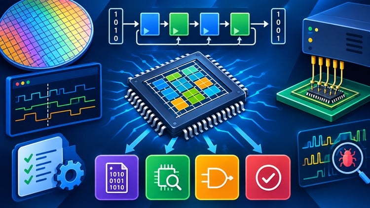
200+ DFT Practice Questions: Scan Design, ATPG, Memory & Logic BIST, Boundary Scan, and Test Coverage
What You Will Learn:
- Master core DFT concepts: fault models, controllability/observability, scan design, and ATPG fundamentals used in real chip design flows
- Understand Memory BIST, Logic BIST, and boundary scan (JTAG/IEEE 1149.1) architectures used to test embedded memories, logic, and I/O
- Apply test compression, fault coverage, and DPPM/defect-level concepts to evaluate and optimize real-world test strategies
- Build confidence with at-speed testing, IDDQ, core-based test (IEEE 1500), and DFT power considerations through practice questions
The Reality Check: Why This DFT Prep Actually Matters
If you’ve been in the VLSI circuit for more than a minute, you know that Design for Testability (DFT) isn’t just a “nice-to-have” anymore—it’s the backbone of modern silicon reliability. I’ve seen brilliant RTL designers crumble in interviews because they couldn’t explain the nuances of test compression or why a specific fault model was failing in silicon. That’s where ‘DFT Interview Preparation and Practice Tests’ steps in. It’s not your typical academic deep dive that puts you to sleep; it’s a focused, high-intensity certification prep tool designed to bridge the gap between “I’ve heard of JTAG” and “I can architect a boundary scan strategy for a multi-core SoC.”
What I appreciate most about this course is its “no-fluff” approach. In an industry where career growth often hinges on passing rigorous technical rounds at companies like NVIDIA, Qualcomm, or Intel, having a repository of 200+ practice questions is a godsend. It feels like a veteran lead engineer is grilling you, forcing you to think about DPPM (Defective Parts Per Million) and at-speed testing from a production standpoint rather than just a theoretical one. It’s about building job-ready skills that translate directly to the Linux terminal and the ATE (Automatic Test Equipment) floor.
Prerequisites: What You Need in Your Toolkit
Before you jump into these practice tests, don’t expect to be spoon-fed the basics of binary. You need a solid foundation to make this worth your time. Here’s the baseline:
- A strong grasp of Digital Logic Design (FSMs, setup/hold time, and combinational logic are non-negotiable).
- Basic familiarity with Verilog or SystemVerilog, as you’ll need to visualize how scan chains are inserted into the RTL.
- An understanding of the VLSI design flow—knowing where Synthesis ends and Physical Design begins helps contextualize where DFT fits in.
- While not mandatory, having a peek at industry-standard tools manuals (like Tessent or Modus) will help you visualize the concepts discussed.
Skills Gained & Industry Tools Context
While this course is primarily question-based, it forces you to master the logic behind the tools. You aren’t just memorizing answers; you’re learning how to evaluate test coverage and optimize ATPG (Automatic Test Pattern Generation) runs. You’ll walk away with a deep understanding of:
- Scan Design & Compression: Learning how to minimize tester time without sacrificing fault coverage.
- BIST Architectures: Deep dives into Memory BIST (MBIST) and Logic BIST (LBIST), which are critical for automotive and high-reliability chips.
- Standard Compliance: Mastering IEEE 1149.1 (JTAG) and IEEE 1500 (Core-Based Test), which are the “languages” of chip communication.
- Power-Aware DFT: Understanding how to manage DFT power considerations so you don’t fry the chip during the shift cycles on the tester.
Career Benefits & Job Roles
Is this a magic bullet? No. But is it a significant catalyst for career growth? Absolutely. The DFT Engineer role is notoriously hard to fill, and companies are willing to pay a premium for candidates who demonstrate real-world project mentalities. Completing this prep puts you on the fast track for roles such as:
- DFT Design Engineer: Implementing scan, MBIST, and JTAG at the RTL level.
- Test/Product Engineer: Using IDDQ and at-speed patterns to debug silicon on the bench.
- Post-Silicon Validation Engineer: Bridging the gap between design intent and actual hardware performance.
- SoC Integration Lead: Managing core-based test strategies for massive 5nm/3nm designs.
What I Liked (The Pros)
- High-Quality Question Bank: The 200+ questions aren’t entry-level “What is a flip-flop?” types. They challenge your understanding of controllability and observability in complex scenarios.
- Focus on DPPM and Defect Levels: I love that it includes the math behind test strategies. Knowing how to calculate the impact of coverage on quality is what separates a junior from a senior engineer.
- Efficient Revision: If you have an interview in three days, this is the best way to stress-test your knowledge. It’s like a simulated hands-on lab for your brain.
- Niche Coverage: It’s rare to find good practice material on IEEE 1500 and IDDQ testing in one place; this course nails the variety.
The Reality Check (The Cons)
- Lack of Tool Simulation: While the theory is top-tier, I would have loved to see some hands-on labs using open-source tools or screenshots from industry-standard tools to help visual learners connect the questions to the actual software environment. It’s very “test-heavy,” so you’ll need to supplement this with your own practical tool experience.